简介
在汽车电子系统的信息安全应用中,多核芯片的核间通信至关重要。瑞萨RH850系列MCU采用了主核(PE)与安全核(ICUM)的双核架构,两者如何高效、可靠地进行数据交换与任务同步?本文将以RH850 P1x-C芯片ICUM与PE核间中断建立为例,深入浅出地讲解其核心原理与配置步骤。
In automotive Cyber Security applications, inter-core communication in multi-core chips is crucial. The Renesas RH850 series MCUs feature a dual-core architecture with a main core (PE) and a security core (ICUM). How do they efficiently and reliably exchange data and synchronize tasks? This article uses the establishment of interrupts between ICUM and PE of the RH850 P1x-C as an example to explain the core principles and configuration steps in an easy-to-understand manner.
1 核间中断的两种跳转方式TWO METHODS FOR INTER-CORE INTERRUPT VECTORING
当PE核需要触发ICUM核的中断(反之亦然),CPU如何找到对应的处理程序?RH850提供了两种方式:直接向量法 (Direct Vector Method) 和表引用法 (Table Reference Method)。
When the PE core needs to trigger an interrupt on the ICUM core (or vice versa), how does the CPU find the corresponding handler? The RH850 provides two methods: Direct Vector Method and Table Reference Method.
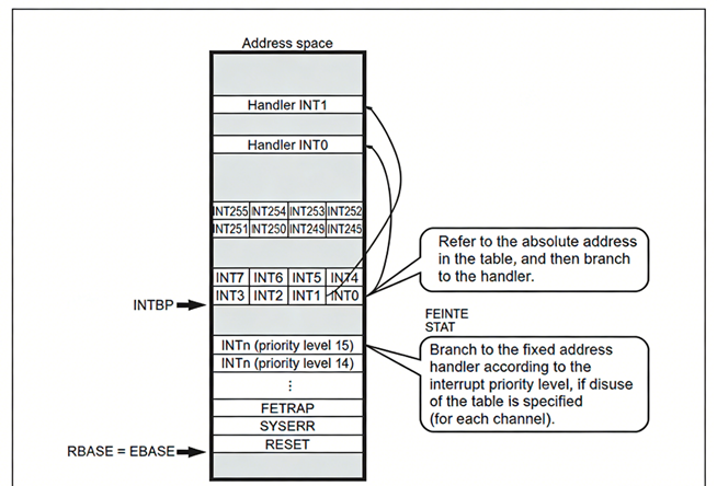
直接向量法:中断处理程序的地址由基地址(Base Address)加上固定偏移量计算得出。基地址由 PSW.EBV 位决定(选择 RBASE 或 EBASE 寄存器),而偏移量则由 RINT 位控制(通常为 0x100)。这种方法简单直接,适用于中断源较少或优先级固定的场景。
Direct Vector Method: The address of the Interrupt Service Routine (ISR) is calculated as Base Address + Offset Address. The base address is selected by the PSW.EBV bit (choosing the RBASE or EBASE register), and the offset is controlled by the RINT bit (typically 0x100). This method is straightforward, suitable for scenarios with fewer interrupt sources or fixed priorities.
可以用以下公式来进行计算:
The following formula can be used for calculation:
Exception Handler Address = base address + offset address
base address:在 PSW.EBV 位中选择是使用 RBASE 寄存器还是 EBASE 寄存器作为基地址。当 PSW.EBV 位被设置为 1 时,使用 EBASE 寄存器的值作为基地址。当 PSW.EBV 位被清零为 0 时,使用 RBASE 寄存器的值作为基地址。
base address:In the PSW.EBV bit, choose whether to use the RBASE register or the EBASE register as the base address. When the PSW.EBV bit is set to 1, the value of the EBASE register is used as the base address. When the PSW.EBV bit is cleared to 0, the value of the RBASE register is used as the base address.
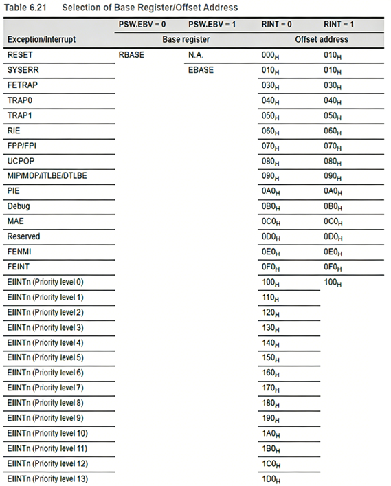
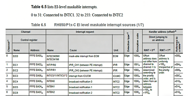
offset address:如果 RBASE.RINT 位或 EBASE.RINT 位被设置为 1,则所有用户中断都使用 100H 的偏移量进行处理。如果该位被清零为 0,则代表使用表引用法。偏移地址根据下表来确定
offset Address: If the RBASE.RINT bit or EBASE.RINT bit is set to 1, all user interrupts will be processed using an offset of 100H. If this bit is cleared to 0, it indicates the use of table reference method. The offset address is determined according to the following table.
对于直接向量方法,每个中断优先级都有一个用户中断异常处理程序,具有相同优先级的多个中断分支会指向同一中断处理程序,如果希望从一开始就为每个中断处理程序使用不同的代码区域,可以通过Table Reference Method解决。
For the direct vector method, each interrupt priority has a user interrupt exception handler. Multiple interrupt branches with the same priority will point to the same interrupt handler. If it is desired to use different code regions for each interrupt handler from the very beginning, the Table Reference Method can be used to solve this problem.
表引用法:中断处理程序的地址存储在一个中断向量表中。CPU通过 INTBP 寄存器(中断表基址指针)加上中断通道号乘以4(INTBP + channel × 4)来读取表中的地址,然后跳转执行。这种方式更为灵活,允许为每个中断通道指定独立的处理函数。
Table Reference Method: The ISR addresses are stored in an interrupt vector table. The CPU reads the address from the table using the INTBP register (Interrupt Table Base Pointer) plus the interrupt channel number multiplied by 4 (INTBP + channel × 4), then jumps to it. This method is more flexible, allowing independent handlers for each interrupt channel.
可以用以下公式来进行计算:
The following formula can be used for calculation:
Exception Handler Address = INTBP register value + EI level maskable interrupt channel number * 4
2 中断注册INTERRUPT REGISTRATION
核间通信需要两条“通道”:一条从PE到ICUM,一条从ICUM到PE。
Inter-core communication requires two "channels": one from PE to ICUM, and one from ICUM to PE.
PE 到 ICUM:使用 EIINT0 中断。需要在ICUM端的异常处理文件(如 exception.850)中注册该中断,并将其与处理函数绑定。当中断触发时,ICUM会先判断中断源,然后调用预先注册的回调函数执行具体功能。
PE to ICUM: Uses the EIINT0 interrupt. You need to register this interrupt in the ICUM's exception handling file (e.g., exception.850) and bind it to a handler function. When the interrupt triggers, the ICUM first identifies the source and then calls the pre-registered callback function.
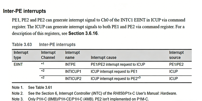
ICUM 到 PE:使用 EIC3 中断。在PE端的启动文件中注册该中断,并指定其处理函数。根据上文所述,使用表引用法时,其向量在表中的偏移量为 0x0C。
ICUM to PE: Uses the EIC3 interrupt. Register this interrupt in the startup file at the PE end and specify its handling function. According to the above description, when using the table reference method, the offset of the vector in the table is 0x0C.
3 中断使能INTERRUPT ENABLE
注册完成后,必须使能中断,通信才算真正准备就绪。使能过程分为几个关键步骤:
After registration, interrupts must be enabled for communication to be truly ready. The enabling process involves several key steps。
1. 使能整体中断掩码:
PE到ICUM:设置 PE2ICUIE 寄存器中对应的位为 1。
ICUM到PE:设置 ICU2PEIE 寄存器中对应的位为 1。
2. 配置中断控制寄存器:为中断设置优先级(Priority)和确认中断向量选择方法(TBn位)。同时,必须将对应的掩码位(MKn)清零,以取消对该中断的屏蔽。
3. 清除CPU级中断掩码:操作 IMR(中断掩码寄存器),将对应中断的掩码位置 0。
4. 全局使能中断:最后,调用 ENABLE_INTERRUPT() 等类似函数,开放CPU的中断总开关。
1. Enable global interrupt mask:
From PE to ICUM: Set the corresponding bit in the PE2ICUIE register to 1.
From ICUM to PE: Set the corresponding bit in the ICU2PEIE register to 1.
2. Configure EIC registers: Set the priority (Priority) and the method for selecting the interrupt vector (TBn bit) for the interrupt. At the same time, the corresponding mask bit (MKn) must be cleared to cancel the masking of this interrupt.
3. Clear CPU-level interrupt mask: Perform the operation on the IMR (Interrupt Mask Register), set the mask position of the corresponding interrupt to 0.
4. Enable interrupts globally: Finally, call functions such as ENABLE_INTERRUPT() to open the overall interrupt switch of the CPU.
4 中断触发INTERRUPT TRIGGER
配置完成后,软件可以通过向特定寄存器写“1”来软件触发一个核间中断。
Once configured, software can trigger an inter-core interrupt by writing a "1" to a specific register.
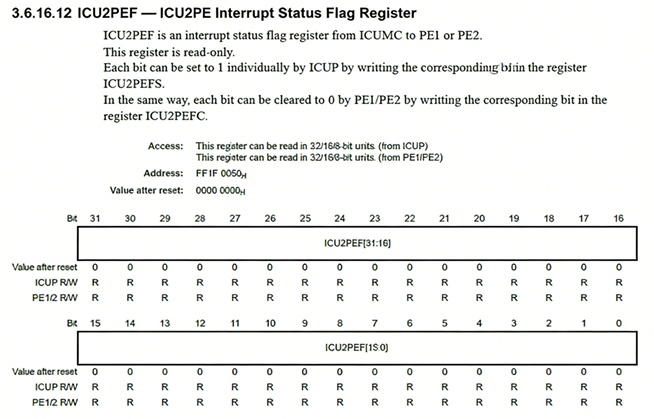
ICUM 触发 PE 中断:向ICU2PEFS寄存器对应位置写1。
ICUM triggers PE interrupt:Write 1 to the corresponding position of the ICU2PEFS register
PE 触发 ICUM 中断:向PE2ICUFS寄存器对应位置写1。
PE triggers ICUM interrupt:Write 1 to the corresponding position of the PE2ICUFS register
5 权限控制ACCESS CONTROL
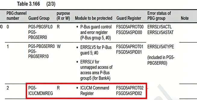
在尝试读写上述控制寄存器时,如果发现无法写入,通常是PBG(外设总线保护)权限未开启。PBG是一种硬件保护机制,防止未授权的访问破坏关键配置。
If you find you cannot write to the control registers mentioned above, it is often because the PBG (Peripheral Bus Guard) permissions are not enabled. PBG is a hardware protection mechanism that prevents unauthorized access from corrupting critical configurations.
例如,ICU_CMDREG 属于 PBG5 保护组。要开启PE核对其的访问权限,需要配置相应的保护寄存器(如 FSGD5APROT02 和 FSGD5APROT03),将对应 PEID 的权限位置 1。
For example, ICU_CMDREG belongs to the PBG5 protection group. To grant the PE core access, you need to configure the corresponding guard registers (e.g., FSGD5APROT02 and FSGD5APROT03) and set the permission bit for the corresponding PEID to 1.
通过以上五个步骤,开发者就能在RH850 P1x-C的双核之间建立起一条稳定、安全的“通信桥梁”。这种核间中断机制是实现安全启动、安全诊断、安全升级等复杂功能的基础,确保了主核与安全核可以协同工作,共同守护车辆的信息安全。
Through the five steps outlined above,developers can establish a stable and secure "communication bridge" between the dual cores of the RH850 P1x-C. This inter-core interrupt mechanism is the foundation for implementing complex functions like Secure Boot, Secure Diagnostics, and Secure Update, ensuring the main core and the security core can work together to safeguard the vehicle's cybersecurity.