1 引言
随着汽车电子电气架构向集中化、网联化、智能化演进,车载控制器的信息安全已从附加特性变为核心需求,是保障车辆功能安全、数据主权与用户隐私的基石。瑞萨电子(Renesas)推出的RH850/P1x-C系列微控制器(MCU)凭借其高性能多核架构与集成化的硬件安全模块(HSM/ICU-M),已成为汽车底盘、动力及先进车身控制器的主流平台。该平台不仅在运行时提供加密、认证与隔离保护,其调试接口与流程本身也嵌入了基于芯片级硬件安全机制(如OCDID认证)的严密设计,有效防止固件泄露、IP盗取及非授权代码注入。
With the evolution of automotive electronic and electrical architecture towards centralization, networking, and intelligence, the information security of in vehicle controllers has shifted from an additional feature to a core requirement, serving as the cornerstone for ensuring vehicle functional safety, data sovereignty, and user privacy. The RH850/P1x-C series microcontrollers (MCUs) launched by Renesas have become the mainstream platform for automotive chassis, power, and advanced body controllers due to their high-performance multi-core architecture and integrated hardware safety module (HSM/ICU-M). The platform not only provides encryption, authentication, and isolation protection during runtime, but its debugging interface and process are also embedded with a rigorous design based on chip level hardware security mechanisms (such as OCDID authentication), effectively preventing firmware leakage, IP theft, and unauthorized code injection.
在量产与售后维护阶段,如何在确保系统整体安全性的前提下,对已部署安全保护机制的控制器进行授权调试,是工程实践中的关键难题。传统的调试接口管理方式往往与最终的安全策略存在矛盾。为解决此问题,知从提出并实现了一种基于服务化接口的安全调试方案。该方案通过在RH850/P1x-C芯片的主核与ICU-M核之间构建标准化的安全调试服务接口(如IcumIf_JtagPwd_Enable、IcumIf_JtagPwd_Disable),将调试接口的使能与关闭操作封装为可控、可审计的安全服务。其核心是运用芯片提供的片上调试ID硬件认证机制,通过向特定地址(如RH850 P1X-C芯片的0xFF280050与0xFF2800B0)写入认证密钥,动态管理调试接口的访问权限,从而在开发调试便利性与产品生命周期安全之间取得最佳平衡。
How to authorize and debug controllers with deployed security protection mechanisms while ensuring overall system security during mass production and after-sales maintenance is a key challenge in engineering practice. The traditional debugging interface management method often conflicts with the final security strategy. To address this issue, ZC proposed and implemented a secure debugging solution based on service-oriented interfaces. This solution constructs a standardized secure debugging service interface (such as IcumIf_JtagPwd_Enable, IcumIf_JtagPwd_Disable) between the main core of RH850/P1x-C chip and the ICU-M core, encapsulating the enable and disable operations of the debugging interface into controllable and auditable secure services. Its core is to use the on-chip debugging ID hardware authentication mechanism provided by the chip, dynamically manage the access permissions of the debugging interface by writing authentication keys to specific addresses (such as 0xFF280050 and 0xFF28000B0 of RH850 P1X-C chip), thus achieving the best balance between development and debugging convenience and product lifecycle security.
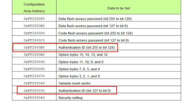
RH850 P1X-C芯片的安全调试机制基于片上调试ID(On-Chip Debug ID, OCDID)硬件认证机制实现。该机制要求在调试器连接时,必须通过预先设置的OCDID进行身份验证,方可开启调试接口的访问权限。实现该功能的关键,在于准确掌握OCDID在芯片内存映射中的存储地址及其编程方法。
The secure debug mechanism of RH850 P1X-C chip is implemented based on the On Chip Debug ID (OCDID) hardware authentication mechanism. This mechanism requires authentication through pre-set OCDID when the debugger connects, in order to grant access to the debugging interface. The key to implementing this function lies in accurately mastering the storage address and programming method of OCDID in the chip memory mapping.
通过对RH850/P1x-C系列芯片技术手册的解析,确认P1X-C型号芯片的OCDID存储地址分为两段独立配置:
第一段配置地址:0xFF280050
第二段配置地址:0xFF2800B0
需向上述两段地址分别写入相应的128位认证密钥,方可完整配置OCDID。该配置通常需在芯片初始化阶段,通过特定的安全服务或底层驱动函数完成。
Through the analysis of the RH850/P1x-C series chip technical manual, it is confirmed that the OCDID storage address of the P1X-C model chip is divided into two independent configurations:
First section configuration address: 0xFF280050
Second section configuration address: 0xFF2800B0
To fully configure OCDID, corresponding 128 bit authentication keys need to be written to the two addresses mentioned above. This configuration usually needs to be completed during the chip initialization phase through specific security services or underlying driver functions.
在知从的设计方案中,安全调试功能的启用与禁用机制通过诊断通信协议进行远程管理。具体而言,设计了两个专用的诊断服务:
服务 0x31 0xFFBB:此服务用于启用调试接口。当通过CAN总线接收到此诊断请求报文时,系统将调用安全服务接口 IcumIf_JtagPwd_Enable()。该函数内部执行逻辑为,通过发送的20字节MasterPassWord,生成32字节SecureJtagPassWord,向芯片指定的OCDID配置地址(0xFF280050与 0xFF2800B0)写入生成的SecureJtagPassWord,从而激活基于OCDID的调试访问认证机制。此后,调试器(如iSYSTEM)连接时必须提供匹配的密钥方可建立调试会话。
服务 0x31 0xFFCC:此服务用于禁用调试接口。当接收到此诊断请求时,系统将调用安全服务接口 IcumIf_JtagPwd_Disable()。该函数执行的操作是通过发送的20字节MasterPassWord,同样通过核间通信将数据发送到ICUM核,在ICUM核生成32字节SecureJtagPassWord,并与芯片中设置的OCDID进行比较,如果比较成功则向上述OCDID地址写入默认值(如全F),以清除已配置的密钥,从而关闭调试接口的认证保护,或将其恢复至默认无效状态。
In the design scheme of ZC, the enabling and disabling mechanism of security debugging function is remotely managed through diagnostic communication protocol. Specifically, two dedicated diagnostic services have been designed:
Service 0x31 0xFBBB: This service is used to enable the debugging interface. When receiving this diagnostic request message through the CAN bus, the system will call the security service interface IcumIf_JtagPwd_Enabling (). The internal logic of this function is as follows: Using the 20-byte MasterPassWord sent, the PE will send it via inter-core communication to the ICUM core. The ICUM core will generate a 32-byte SecureJtagPassWord, and write the generated SecureJtagPassWord to the specified OCDID configuration address (0xFF280050 and 0xFF2800B0) of the chip, thereby activating the debugging access authentication mechanism based on the OCDID. Thereafter, the debugger (such as iSYSTEM) must provide a matching key when connecting to establish a debugging session.
Service 0x31 0xFCCC: This service is used to disable the debugging interface. When receiving this diagnostic request, the system will call the security service interface IcumIf_JtagPwd_Disab(). The operation performed by this function is to send the 20-byte MasterPassWord, and simultaneously send the data to the ICUM core through inter-core communication. In the ICUM core, a 32-byte SecureJtagPassWord is generated and compared with the OCDID set in the chip. If the comparison is successful, the default value (such as all Fs) will be written to the above OCDID address to clear the configured key, thereby disabling the authentication protection of the debugging interface or restoring it to the default invalid state.
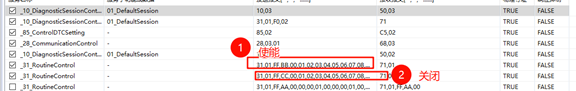
此设计将底层的芯片安全调试硬件控制(OCDID配置)封装为标准化的、可远程调用的诊断服务,实现了调试权限的按需、可控管理,显著提升了在量产部署和售后维护场景下进行授权诊断与调试的安全性和便利性。
This design encapsulates the underlying chip security debugging hardware control (OCDID configuration) into standardized, remotely callable diagnostic services, achieving on-demand and controllable management of debugging permissions, significantly improving the security and convenience of authorized diagnosis and debugging in mass production deployment and after-sales maintenance scenarios.
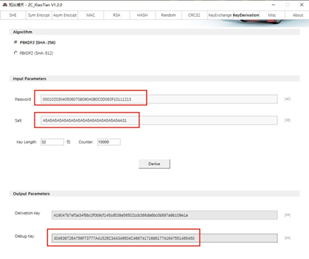
在通过诊断服务 0x31 0xFFBB启用安全调试功能后,调试器(如 iSYSTEM winIDEA)连接芯片时必须通过OCDID认证,即输入正确的32字节SecureJtagPassWord。该密码并非明文存储,而是由受保护的20字节MasterPassWord通过特定算法派生得出,以确保根密钥的安全性。
After the security debugging function is enabled through the diagnostic service 0x31 0xFFBB, the debugger (such as iSYSTEM winIDEA) must pass OCDID authentication when connecting to the chip, that is, enter the correct 32 byte SecureJTagPassWord. The password is not stored in plain text, but is derived from a protected 20 byte MasterPassWord using a specific algorithm to ensure the security of the root key.
密钥派生与获取可以通过知从啸天工具来获取:输入20字节的MasterPassWord到PassWord,然后输入预设的Salt值,设置好Key Length,就可以得到派生好的SecureJtagPassWord。
Key derivation and acquisition can be obtained through the ZC XiaoTian tool: enter a 20 byte MasterPassWord into PassWord, then enter the preset Salt value, set the Key Length, and you can obtain the derived SecureJtagPassWord.