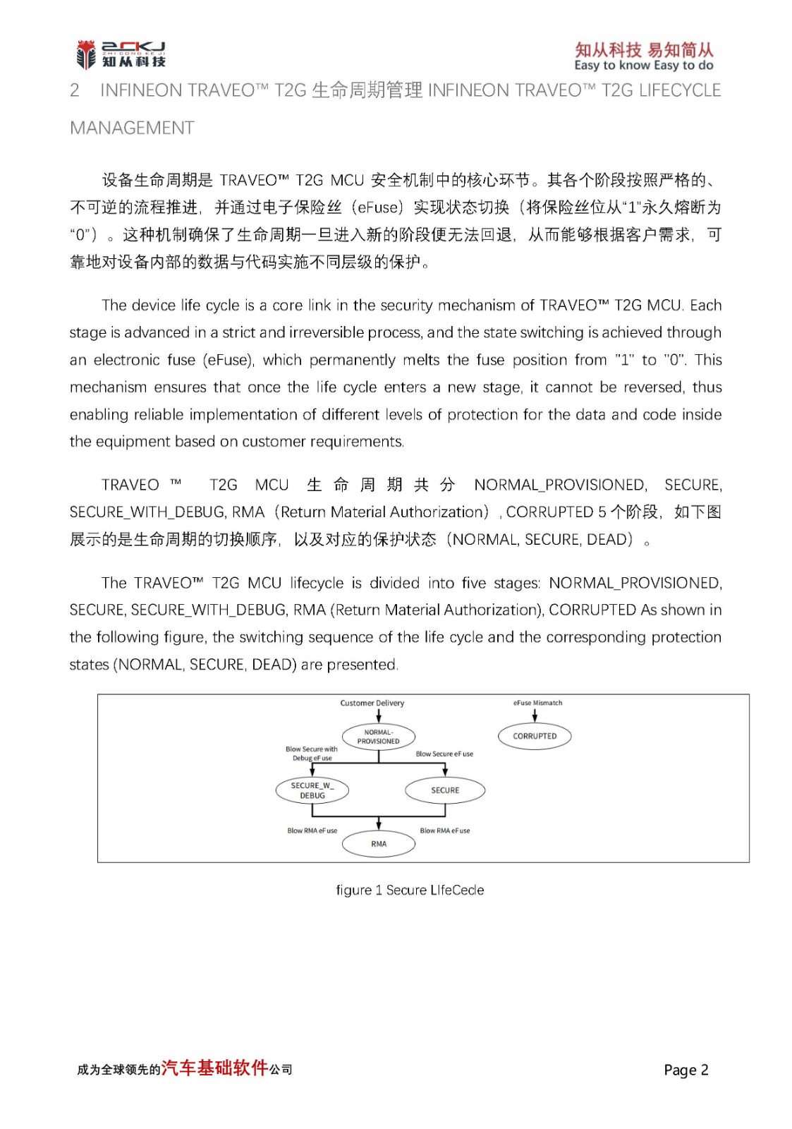
1 项目背景 Introduction
在嵌入式安全通信领域,AES-CMAC(RFC 4493)是报文完整性校验的核心算法之一。本文记录了在瑞萨 RH850 P1H-C(R7F701372)平台上,利用 ABCA0 硬件加速器对 aes_cmac() 函数进行五轮深度性能优化的完整过程——从原始的 1.2 秒,最终压缩至 90 毫秒,实现 约 13 倍的整体性能提升。
In the field of embedded secure communication, AES-CMAC (RFC 4493) is one of the core algorithms for message integrity verification. This paper documents the complete process of conducting five rounds of in-depth performance optimization for the aes_cmac() function using the ABCA0 hardware accelerator on the Renesas RH850 P1H-C (R7F701372) platform—reducing the original 1.2 seconds to 90 milliseconds, achieving approximately a 13-fold overall performance improvement.
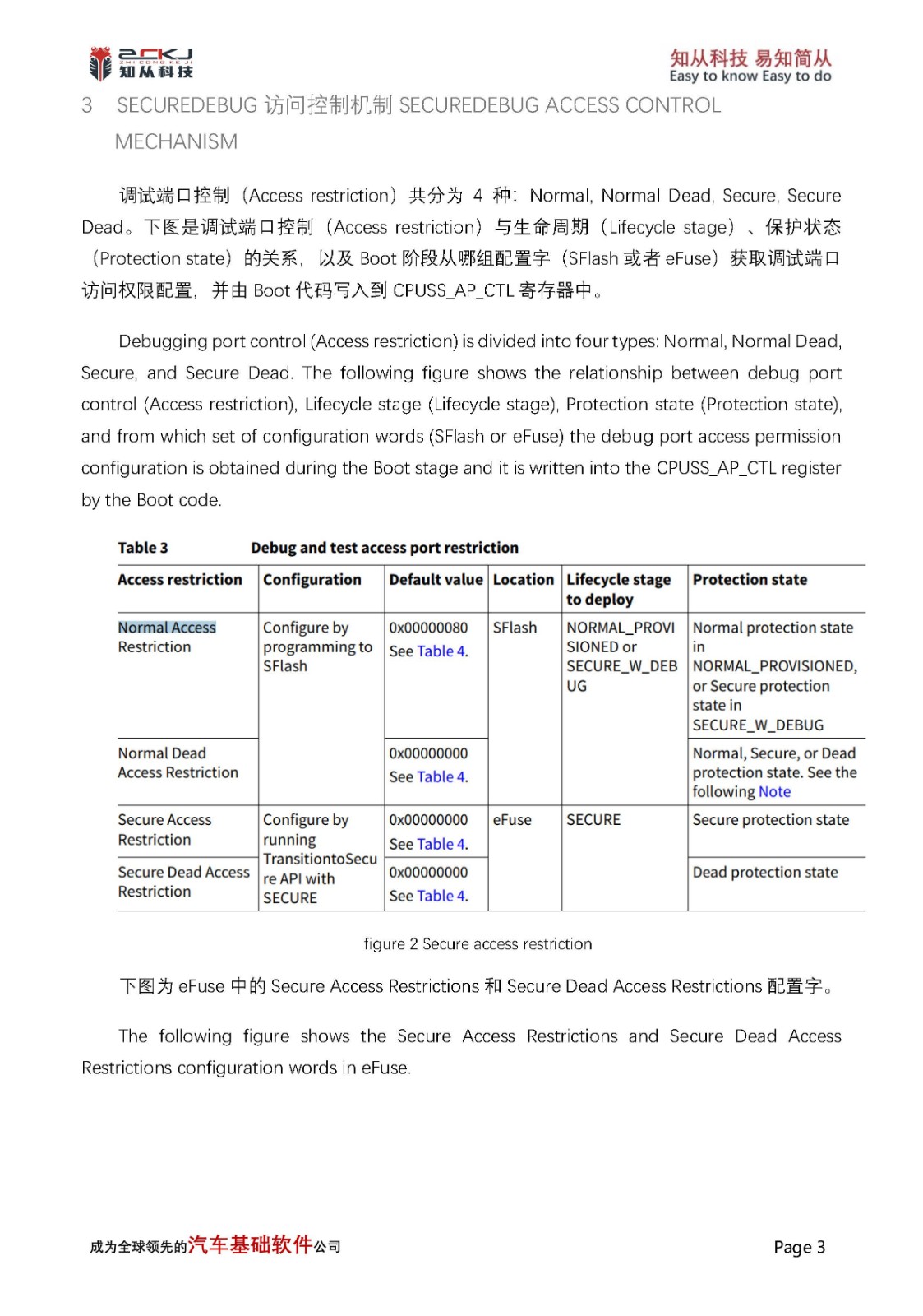
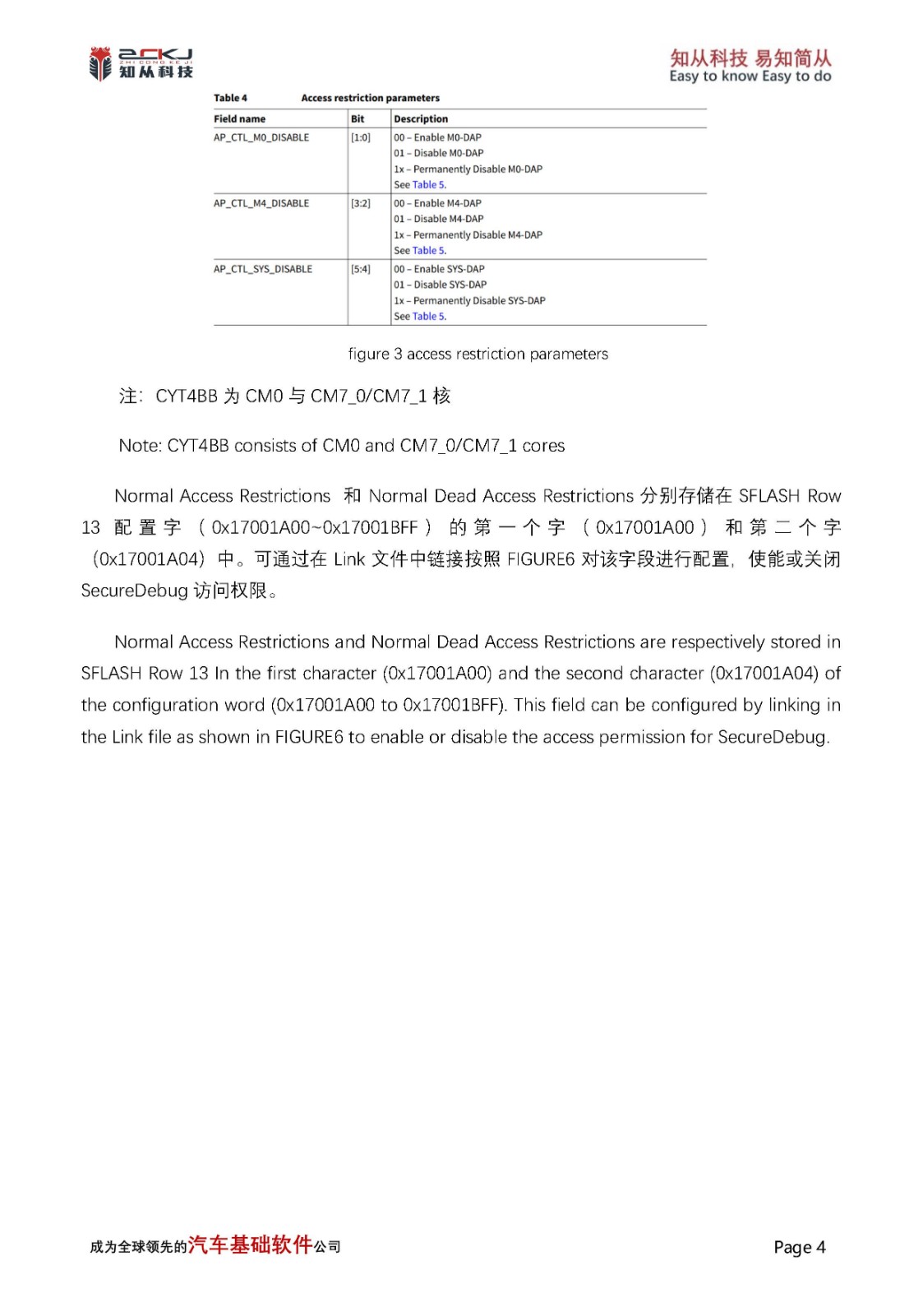
2 算法原理简述 Design of Security Debugging Function
AES-CMAC 的核心是一个 CBC-MAC 变体,对输入数据按 16 字节分块,逐块执行 XOR → AES-ECB 加密 的链式运算。最后一块根据填充情况选择不同的子密钥(subkey_1 或 subkey_2)参与异或。
The core of AES-CMAC is a variant of CBC-MAC, which processes input data in 16-byte blocks, performing a chained operation of XOR followed by AES-ECB encryption. The final block selects different subkeys (subkey_1 or subkey_2) for XOR based on the padding scenario.
M₁ ⊕ IV → AES → X₁
M₂ ⊕ X₁ → AES → X₂
M₃ ⊕ X₂ → AES → X₃ ← 最终 MAC
算法本身是串行的——每一块的输出是下一块的输入——因此无法通过并行化加速。优化空间全部集中在 减少每块的 CPU 侧指令开销 和 最小化硬件交互轮次 上。
The algorithm itself is sequential—each block's output serves as the input for the next block—thus, it cannot be accelerated through parallelization. The optimization potential lies entirely in reducing CPU-side instruction overhead per block and minimizing hardware interaction rounds.
3 性能基线分析Design of Security Debugging Function
原始实现中,aes_cmac() 在循环内对每一块调用 R_AES_HW_ECB_Encrypt(),而该函数每次都会完整执行初始化流程:
In the original implementation, aes_cmac() calls R_AES_CW-ECBEncrypt() on each block within the loop, and this function executes the initialization process completely each time:
每块执行: Init → Configure → LoadKey → ProcessBlock
原始每块指令分解:
操作 | 指令数(估) | 说明 |
R_AES_HW_ECB_Encrypt 函数调用/返回 | 10 | call/ret + 参数传递 |
R_AES_HW_Init | 15 | 每块检查 s_initialized + wait |
R_AES_HW_Configure | 20 | 参数校验 + MD 寄存器写入 |
R_AES_HW_LoadKey | 60 | bytes_to_words(~45) + di/ei + CTL + IDAT + wait |
R_AES_HW_ProcessBlock | 90 | bytes_to_words(~45) + di/ei + CTL + IDAT + wait + di/ei + ODAT + words_to_bytes(~45) |
aes_cmac循环 block_xor_triple 调用 | 16 | 函数调用 + 4×XOR |
aes_cmac 循环: if/else if 分支 | 6 | 每块判断 last block |
总计 | 250+ |
APP 数据 CMAC 计算实测耗时:1.2 秒。
APP data CMAC calculation actual measurement time: 1.2 seconds.
4 优化过程Design of Security Debugging Function
4.1 第 1 轮:循环外一次性完成硬件初始化 Complete hardware initialization in one go outside the loop
问题分析 Problem analysis :
R_AES_HW_ECB_Encrypt() 每次调用都执行 Init + Configure + LoadKey,但这些操作的结果在连续的 CMAC 运算中是不变的——密钥不变,模式不变,硬件只需配置一次。
Each call to R_AES-HW-ECBEncrypt() executes Init+Configure+LoadKey, but the results of these operations remain unchanged in continuous CMAC operations - the key remains unchanged, the mode remains unchanged, and the hardware only needs to be configured once.
改动modify:
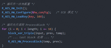
效果effect:
每块消除 Init(~15) + Configure(~20) + LoadKey(~60) = ~95 条指令。
实测时间:1.2 s → 0.75 s,提升约 1.6×。
Each block eliminates approximately 95 instructions, including Init (~15), Configure (~20), and LoadKey (~60).
Actual testing time: 1.2 s → 0.75 s, with an increase of approximately 1.6 times.
要点key points:
这是最"显而易见"的优化,但很多基于硬件加速器的加密库默认就是逐块完整初始化的——原因通常是安全性考量(防止密钥残留)或 API 简洁性。在裸机可控环境下,循环外初始化是安全且收益显著的第一步。
This is the most obvious optimization, but many hardware accelerator based encryption libraries default to complete initialization block by block - usually due to security considerations (preventing key residue) or API simplicity. In a controllable bare metal environment, out of loop initialization is a safe and profitable first step.
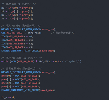
4.2 第 2 轮:bytes↔words 转换优化 bytes ↔ Words Conversion Optimization
问题分析 Problem analysis:
R_AES_HW_ProcessBlock() 内部的处理流程为:
The internal processing flow of R_AES_CrocessBlock() is as follows:
bytes → bytes_to_words() → 写 IDAT 寄存器 → HW 加密 → 读 ODAT 寄存器 → words_to_bytes() → bytes
其中 bytes_to_words() 和 words_to_bytes() 各约 45 条指令,合计 ~90 条指令——是为了将 16 字节数组与 ABCA0 的 32 位寄存器接口适配。
RH850 是小端(Little-Endian)架构。对于 4 字节对齐的 uint32 指针,直接内存读取的结果与手动拼接完全等价:
Among them, bytes_to-words() and words_to-bytes() each have about 45 instructions, totaling~90 instructions - in order to adapt the 16 byte array to the 32-bit register interface of ABCA0.
RH850 is a Little Endian architecture. For a 4-byte aligned uint32 pointer, the result of direct memory reading is completely equivalent to manual concatenation:
/* C 语言手动拼接 */
uint32 val = bytes[0] | (bytes[1]<<8) | (bytes[2]<<16) | (bytes[3]<<24);
/* 小端平台上直接读取 */
uint32 val = *(uint32 *)(bytes); /* 结果完全相同 */
改动modify:
将 bytes_to_words 和 words_to_bytes 用 RH850 汇编重写,充分利用 RH850 的 32 位 load/store 指令,消除逐字节移位拼接:
Rewrite bytes_to-words and words_to-bytes using RH850 assembly, fully utilizing RH850's 32-bit load/store instruction to eliminate byte by byte shift concatenation:
; bytes_to_words 汇编版本(示意)
; 利用 ld.w 直接读取 32 位,替代逐字节 shift+or
ld.w r6, 0[r10] ; 直接读 4 字节
st.w r6, 0[r11]
ld.w r6, 4[r10]
st.w r6, 4[r11]
; ...
同时在 aes_cmac.c 中调用改为:
At the same time, change the call in aes_cmac. c to:
R_AES_HW_ProcessBlock_Aligned((const uint32 *)temp, (uint32 *)prev);
效果effect:
每块消除 2 次转换函数 = ~90 条指令。
实测时间:0.75 s → 0.4 s,提升约 1.9×。
Each block eliminates 2 conversion functions=~90 instructions.
Actual testing time: 0.75 s → 0.4 s, with an increase of approximately 1.9 times.
第二轮选择用汇编重写转换函数,而非简单的 C 语言指针强转,原因在于:工程需要保证 严格的数据对齐假设显式化,汇编版本明确控制了 load/store 的地址对齐汇编版本可精确控制指令序列,避免编译器生成多余的 load/store 对在后续优化中,这些汇编片段可以直接内联到更大的优化函数中。
In the second round, we chose to rewrite the conversion function using assembly instead of simple C language pointer rotation. The reason is that the project needs to ensure strict data alignment, and the assembly version explicitly controls the address alignment of load/store. The assembly version can precisely control the instruction sequence and avoid the compiler generating redundant load/store pairs. In subsequent optimizations, these assembly fragments can be directly inline into larger optimization functions.
4.3 第 3 轮:CMAC 主循环下沉到驱动层
问题分析 Problem analysis:
即使使用了汇编优化的 ProcessBlock_Aligned,每块仍存在大量逐块冗余开销,这些开销的本质原因是 抽象层边界切割不当——CMAC 的逐块逻辑(XOR、分支判断、HW 交互)分散在 aes_cmac.c 和 icum_d_aes_hw.c 两个编译单元中,编译器无法跨文件内联和优化。
Even with assembly optimized ProcessBlock_Aligned, there is still a significant amount of block by block redundancy overhead per block, which is essentially due to improper boundary cutting of the abstraction layer - CMAC's block by block logic (XOR, branch decision, HW interaction) is scattered in two compilation units, aes_cmac. c and icum_d_aes_hw. c, making it impossible for the compiler to inline and optimize across files.
改动modify:
核心思路:将整个 CMAC 主循环(XOR → HW ECB → ODAT 读取 → last block 处理)合并为驱动层的单个函数,一次性接收全部参数。
Core idea: Merge the entire CMAC main loop (XOR → HW ECB → ODA read → last block processing) into a single function in the driver layer, receiving all parameters at once.
aes_hw_error_t R_AES_HW_CMAC_ProcessBlocks(
const uint8 *p_input,
uint32 length,
const uint8 *p_subkey1,
const uint8 *p_subkey2,
uint8 *p_mac_out)
(1)函数内部结构 Internal structure of function:
1. 参数检查(仅一次)
2. 计算 n_blocks, remainder, prefix_count
3. 预计算 CTL 值
- ctrl_first = START | NEW_KEY(首块)
- ctrl_rest = 0x0000(后续块)
4. 首块单独处理(循环外),使用 ctrl_first
5. 后续块紧凑循环(无分支),使用 ctrl_rest
6. 最后一块:subkey XOR + padding 处理
1. Parameter check (only once)
2. Calculate n_blocks, residual, prefix_count
3. Pre calculate CTL values
-Ctrlfirst=START | NEW_KEY (first block)
-Ctrd_reset=0x0000 (subsequent block)
4. Process the first block separately (outside the loop) using ctrd_first
5. Compact loop for subsequent blocks (without branches), use ctrd_reset
6. Last block: subkey XOR+padding processing
(2)每块热循环内的实际操作 Actual operation within each thermal cycle:
(3)aes_cmac.c 主循环替换为单次调用 Replace the aes_cmac. c main loop with a single call:
hw_ret = R_AES_HW_CMAC_ProcessBlocks(input, length, subkey_1, subkey_2, mac_value);
if (hw_ret == AES_HW_OK) {
return;
}/* 否则走纯软件回退路径 */
效果effect:
每块消除 ~37 条指令。
实测时间:0.4 s → 0.2 s,提升约 2×。
Eliminate~37 instructions per block.
Actual testing time: 0.4 s → 0.2 s, an increase of about 2 ×.
设计考量 design considerations:
将 CMAC 逻辑下沉到驱动层违背了"驱动只做硬件抽象"的传统分层原则。但在嵌入式性能敏感场景中,这种权衡是合理的:CMAC 是该硬件加速器的主要使用场景,不是边缘用例;裸机环境下没有多进程竞争,不需要严格的抽象隔离;保留了R_AES_HW_ProcessBlock_Aligned() 作为通用接口,其他算法仍可使用。
Downgrading CMAC logic to the driver layer violates the traditional layering principle of 'drivers only do hardware abstraction'. But in embedded performance sensitive scenarios, this trade-off is reasonable: CMAC is the main usage scenario for this hardware accelerator, not an edge use case; There is no multi process competition in a bare metal environment, and strict abstract isolation is not required; Retained R_AES-HW-ProcessBlock_Aligned() as a universal interface, while other algorithms can still be used.
4.4 第 4 轮:循环内 PSW 寄存器读取优化 Optimization of PSW register reading within the loop
问题分析 Problem analysis:
DISABLE_INTERRUPT_WITH_CHECK 宏的展开逻辑:
#define DISABLE_INTERRUPT_WITH_CHECK(saved) do {
saved = STSR(PSW); /* 读系统寄存器 ~3 条指令 */
if (0 == (saved & 0x20)) { /* 条件分支 ~2 条指令 */
__DI(); /* ~1 条指令 */
}
} while(0)
每块执行 2 次(写 IDAT 前 + 读 ODAT 前),仅 STSR(PSW) 就是 ~6 条指令。STSR 是特权系统寄存器读取,开销高于普通内存访问,循环执行期间,PSW.ID 位(中断禁止标志)不会被外部代码改变——裸机环境下没有其他线程会在我们的循环中间修改中断状态。
Each block is executed twice (before writing IDAT+before reading ODAT), and STSR (PSW) alone contains~6 instructions. STSR is a privileged system register read with higher overhead than regular memory access. During loop execution, the PSW.ID bit (interrupt disable flag) will not be changed by external code - no other thread in a bare metal environment will modify the interrupt state in the middle of our loop.
改动modify:
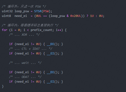
效果effect:
每块消除 2 次 STSR(PSW) = ~8 条指令。
实测时间:0.2 s → 180 ms。
Each block eliminates 2 STSR (PSW)=~8 instructions.
Actual measurement time: 0.2 s → 180 ms.
4.5 第 5 轮:开启编译器优化(-Ospeed)
问题分析 Problem analysis:
经过前四轮的手工优化,CPU 侧的"显性冗余"已被基本消除。此时进一步的手动代码重构收益递减。但回顾整个优化过程,有一个维度始终未被触及——编译器优化级别。工程中 CMAC 和 AES 硬件驱动相关的 .gpj 文件此前可能使用的是默认或较低的优化级别(如 -O0 或 -O1)。编译器在低优化级别下:不进行函数内联(即使在同一编译单元内);不消除冗余的 load/store;不进行循环展开或指令调度;不利用 RH850 的寻址模式优化。
After the first four rounds of manual optimization, the "explicit redundancy" on the CPU side has been basically eliminated. At this point, further manual code refactoring yields diminishing returns. But looking back at the entire optimization process, there is one dimension that has never been touched upon - the compiler optimization level. The. gpj files related to CMAC and AES hardware drivers in engineering may have previously used default or lower optimization levels (such as - O0 or - O1). At low optimization levels, the compiler does not inline functions (even within the same compilation unit); Do not eliminate redundant load/store; Do not perform loop expansion or instruction scheduling; Optimizing the addressing mode without utilizing RH850
改动modify:
对以下 .gpj 文件添加 -Ospeed 编译选项:
CMAC 相关的 .gpj(aes_cmac.c 所在工程文件)
AES 硬件驱动的 .gpj(icum_d_aes_hw.c 所在工程文件)
Add the - OSpeed compilation option to the following. gpj files:
CMAC related. gpj (project file containing aes_cmac. c)
AES hardware driver. gpj (project file containing icum_d_aes_hw. c)
效果effect:
实测时间:180 ms → 90 ms,提升约 2×。
Actual testing time: 180 ms → 90 ms, an increase of about 2 times.
这是五轮优化中 单轮收益最大 的一步,说明前四轮手工优化后的代码中存在一些可被编译器消除的低效模式——特别是函数调用边界处的寄存器保存/恢复、冗余的条件分支、以及循环中的不变量计算。
This is the most profitable step in a single round of optimization among the five rounds, indicating that there are some inefficient patterns in the code after the first four rounds of manual optimization that can be eliminated by the compiler, especially register save/restore at function call boundaries, redundant conditional branching, and invariant computation in loops.
and invariant computation in loops.

 收起
收起

收起