- ZC.QingLong Secureboot Based On Infineon TC2XX
- ZC.QingLong SPI OTA Product Manual Based On Infineon TC397
- ZC.QingLong SecureBoot Product Manual Based on NXP S32K3 For CHERY QSQR
- ZC.QingLong BootLoader Product Manual Based on NXP S32K3
- ZC.QingLong FOTA Solution
- ZC.QingLong BootLoader
- ZC.QingLong BootLoader Product Manual Based on NXP KW45
- ZC.QingLong SecureBoot Product Manual Based on Infineon TC377
- ZC.QingLong FOTA Product Manual Based on Infineon TC387
- Introduction to ZC.QingLong Ethernet Flashing Based on RH850U2A
- ZC.Qinglong Ethernet BootLoader Product Manual Based on RENESAS RH850U2A
- ZC.QingLong SecureBoot Product for NXP S32K344
- ZC.QINGLONG FOTA PRODUCT MANUAL BASED ON INFINEON TLE9893
- ZC.QINGLONG SECUREBOOT PRODUCT MANUAL BASED ON INFINEON TC2XX FOR FAW-VW
- ZC.QINGLONG YUNTU YTM32B1HA0X SECUREBOOT INTRODUCTION
- ZC.QINGLONG UART BOOTLOADER PRODUCT MANUAL BASED ON TMS570
- ZC.QINGLONG PIPELINE PROGRAM SOLUTION INTRODUCTION
- ZC.QingLong BootLoader Based on Infineon TC213 SMTC
- ZC.QingLong BootLoader Product Manual Based on STSPC58NN for GEELY GEEA2.0
- ZC.Qinglong Bootloader Product Manual Based On NXP NCJ29D5
- ZC.QingLong FOTA Product Manual Based on Infineon TC3xx
- ZC.QingLong FOTA
- ZC.QingLong Secureboot Based on NXP S32K1XX
In the traditional bootloader flashing process, data download and data programming follow a strictly serial execution model: the bootloader must wait for an entire data block (e.g., a complete Flash sector) to be fully received and verified via buses like CAN or Ethernet before initiating erase and write operations on the Flash memory. During this period, the high-speed data bus remains idle while waiting for the relatively slow Flash operation to complete, and the Flash memory also sits idle awaiting the next data block. This alternating “wait-busy” pattern results in low hardware resource utilization and significantly extends the overall programming time, becoming a major bottleneck for efficiency improvement.
Queue-based flashing constitutes an efficient firmware update solution for individual ECU controllers. Its core principle lies in breaking the serial dependency between data transmission and Flash programming inherent in conventional flashing methods. By introducing data buffering queues and task overlapping execution mechanisms, both processes are parallelised, thereby significantly reducing overall flashing duration. This approach essentially applies the “queue” concept from computer architecture to the embedded programming domain. It maximises utilisation of bus bandwidth and Flash programming time by trading space for time (sacrificing a small amount of RAM as buffer space). The diagram below illustrates the timing difference between non-queued and queued programming:
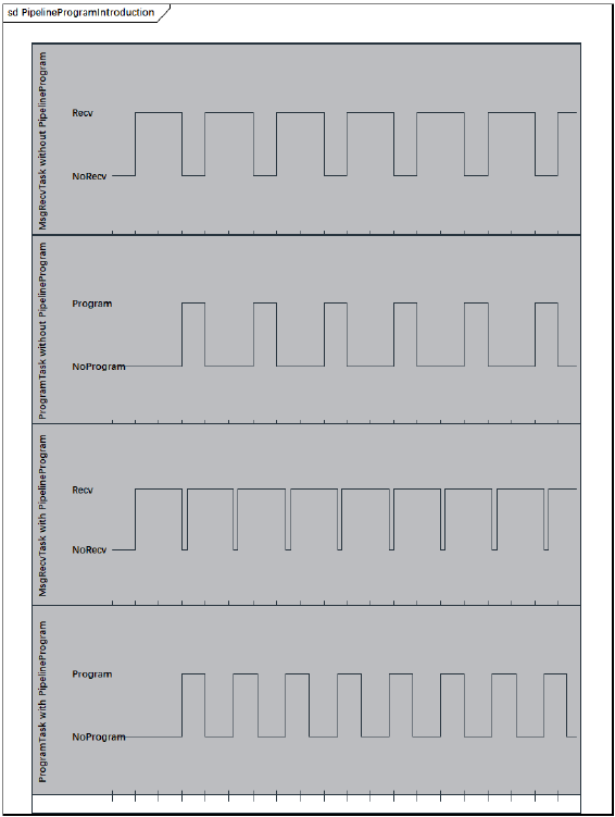
The implementation of the pipeline flashing solution begins with meticulous initial configuration and preparatory work. On the server side, the complete firmware image is pre-partitioned into a series of contiguous, fixed-size data blocks. The block size must be determined by comprehensively considering the physical characteristics of Flash sectors, the single-frame payload limit of the communication protocol, and the available RAM resources within the target ECU, to achieve an optimal balance between transmission efficiency and memory overhead. Simultaneously, within the ECU's Bootloader, at least two independent RAM buffers must be allocated—forming a classic dual-buffer structure—alongside a dedicated state machine to manage the entire flashing lifecycle. The communication protocol requires corresponding enhancements, adding a flow control mechanism to coordinate transmission and reception rhythms on top of standard data download services.
Upon initiating the specific flashing process, the host first transmits the initial data block. The Bootloader stores this data in Buffer A and performs real-time verification. Once Buffer A is filled with valid data and verification succeeds, the core parallel logic of the entire solution activates immediately: The Bootloader sends an acknowledgment to the host and requests the next data block while simultaneously initiating the programming of Buffer A's data into Flash memory. From this point, the system enters a highly efficient pipeline operation: while the host transmits the second data block to Buffer B, the Flash driver independently processes the programming of Buffer A's data. Upon Buffer B's reception completion and Buffer A's programming finish, their roles instantly switch—Buffer B is handed over to Flash for programming, while the newly freed Buffer A prepares to receive the third data block. This cycle repeats, with data reception and Flash programming “ping-ponging” between the two buffers to form a stable relay loop. This enables the communication bus and Flash memory to operate in parallel for extended periods, maximizing resource utilization.
The final phase requires special handling. Upon receiving the last data block, the pipeline completes its final “receive-program” cycle. The Bootloader then ceases requesting new data but must wait for the programming of this final block to fully conclude. Following this, the system performs a final global verification. This includes calculating the CRC checksum for the entire programmed region and comparing it against the authoritative digest provided by the host. This ensures the integrity and correctness of the entire firmware image. Only upon passing this ultimate verification does the Bootloader update metadata such as version information, signifying the safe and successful completion of the pipeline programming task.
Due to variations in hardware and software configurations, employing queue-based write optimisation schemes may yield differing outcomes across environments. Certain usage scenarios may result in failed queue writes or failure to achieve the intended reduction in write latency. The following outlines potential issues encountered when implementing queue-based write optimisation, alongside recommended solutions:
l Queue Stagnation:
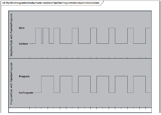
In queue-based flash programming schemes, the expected data write time is typically shorter than the expected data transfer time. However, in practical scenarios, the data write time may significantly exceed the data transfer time. This can rapidly fill the buffer, forcing the host to wait and resulting in poor parallel efficiency. Recommended solutions are as follows:
1. Optimise the Flash driver: Employ a faster write mode.
2. Increase buffer size: Allow reception of more data blocks to compensate for programming delays.
3. Adjust block size: Reduce block size to accelerate programming tasks and enable more frequent buffer clearance.
l Data asynchrony
The queue flashing process involves multiple data handling operations. Errors in buffer switching logic or flag contention may cause data overwriting or incorrect programming, ultimately resulting in failed file verification. Recommended solutions are as follows:
1. Strict critical section protection: Employ interrupt disabling or mutual exclusion locks.
2. State machine validation: Implement multi-condition checks prior to switching.
3. Sequence number incrementation: Append a sequence number to each data block and verify it prior to programming.
As ECU functionality grows increasingly complex, program memory capacity has surged from hundreds of kilobytes to several megabytes or even tens of megabytes. This time-consuming serial approach has become increasingly problematic in production line-off and aftermarket upgrade scenarios. To maximize hardware performance and minimize overall programming time, “pipeline programming” technology emerged. Its core concept involves introducing a data buffer queue (typically a double-ended buffer or circular buffer) to transform linear serial tasks into parallel pipeline operations. Specifically, the Bootloader divides the entire data stream into multiple contiguous data blocks. Upon completing reception of the first block, it immediately initiates Flash programming for that block without waiting for all data. Simultaneously, the background reception process for the second block utilizes bus bandwidth to run in parallel with the programming operation of the previous block. This iterative process creates temporal overlap between “receiving block N+1” and “programming block N.” Consequently, the previously wasted bus idle time and Flash wait time are effectively utilized, partially offsetting the data bus transfer time and Flash programming time. Ultimately, this achieves speed optimization for the single-controller flashing process, yielding particularly significant time savings when handling large-capacity Flash or using relatively low-speed communication interfaces. This technique represents a classic optimization strategy in embedded bootloader design, trading space (buffer) for time (programming duration).
Click to download the product manual