- 知从木牛基础软件OBD
- 知从木牛基础软件英飞凌TC264
- 知从木牛OSEK网络管理恩智浦S32K344
- 知从木牛操作系统OS
- 知从木牛操作系统OS SC4
- TRICORE平台移植到ARM平台指导手册
- 知从木牛操作系统OS ARM CORTEX R52+
- 知从木牛基础软件英飞凌TC4X
- 知从木牛基础软件恩智浦S32K3
- 知从木牛基础软件英飞凌TLE989X
- 知从木牛AFE德州仪器BQ756506
- 知从木牛基础软件瑞萨RH850U2AX
- 知从木牛AUTOSAR软件平台英飞凌TC264
- 知从木牛基础软件杰发AC781X
- 知从木牛操作系统OS NG HYPERVISOR
- 知从木牛基础软件杰发AC7840
- 知从木牛基础软件瑞萨RH850F1KM
- 英飞凌TC3XX_Cache和Overlay功能详解
- 知从木牛基础软件芯旺微KF32A产品手册
- 知从木牛基础软件恩智浦S32K344产品
- 知从木牛基础软件紫光同芯THA6206
- 知从木牛基础软件旗芯微FC7300
- 知从木牛轻量化基础软件平台
- 知从木牛基础软件平台
- 知从木牛AUTOSAR软件平台恩智浦S32K
- 知从木牛AUTOSAR软件平台恩智浦MPC5744P
- 知从木牛AUTOSAR软件平台英飞凌TC275
- 知从木牛SOC产品
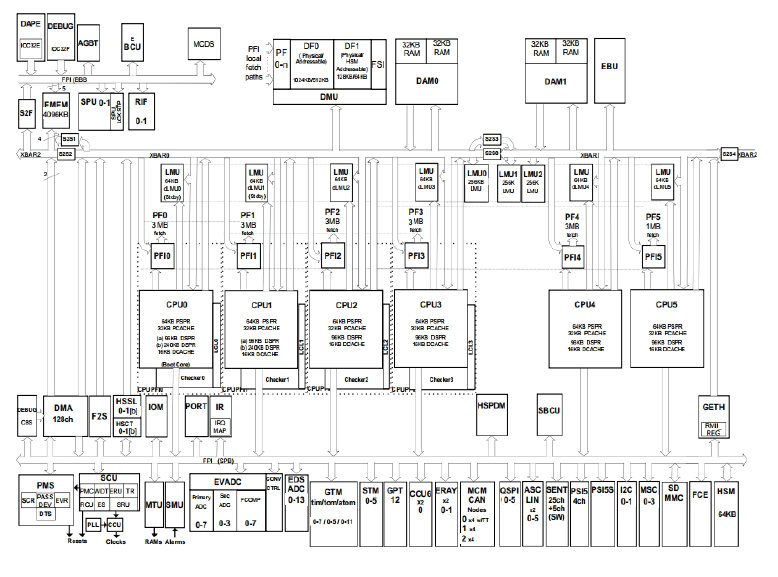
英飞凌AURIX™ TC3XX系列微控制器是面向汽车电子和工业控制领域的高性能多核处理器平台,其架构设计充分考虑了实时性、功能安全(ISO 26262)和信息安全的需求。该系列采用TriCore™异构多核架构,结合了精简指令集计算机(RISC)和复杂指令集计算机(CISC)的特征,整合了32位RISC CPU、DSP运算单元和专用外设控制器,主频可达300MHz,内置HSM(硬件安全模块),在ASIL-D级功能安全认证和信息安全防护方面具有显著优势。在存储子系统设计上,TC3XX创新性地融合了缓存(Cache)机制和数据访问覆盖(Data Access Overlay)技术,有效解决了汽车电子系统中实时数据处理与存储访问效率的关键矛盾。
CACHE模块概述
TC3XX的缓存系统分为PCache(指令缓存)和DCache(数据缓存),Cache内部组成包含Cache控制器和两块SRAM (Tag RAM、DATA RAM)。程序缓存(PCACHE)采用两路组相联的缓存结构,每组有两个缓存行可选,每个缓存行大小为256位。针对汽车电子典型的总线访问模式,缓存控制器使用了最近最少使用算法(LRU)进行缓存替换。因此当缓存满时,替换最长时间未使用的缓存行。在ADAS传感器数据处理场景中可实现较高缓存命中率。
内存空间概述
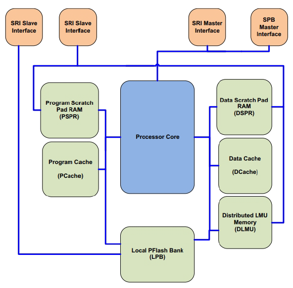
TC3XX采用先进的32位架构,实现了一个全面而复杂的内存系统。其内存空间的设计充分考虑了现代汽车电子系统对高性能、实时性和功能安全的严格要求。整个内存系统采用分层设计理念,包括非易失性存储器(程序闪存和数据闪存)、多级RAM系统(本地SRAM、全局SRAM和局部存储单元LMU)以及A/B分区。这种多层次的存储架构不仅确保了数据访问的高效性,还通过多重保护机制维护了系统的安全性和可靠性。
此外,所有总线主设备都可以在相同地址访问相同的外设和存储器。系统地址映射对所有CPU都是可见且有效的,这意味着所有外设和资源都可以被所有TriCore CPU和其他片上总线主设备访问。当然,也可以借助总线MPU(存储器保护单元)根据需求,配置不同细粒度的访问控制来保护关键的存储器区域。具体来说,MPU包含了三个主要的保护组件:首先是八个读写保护的暂存器存储器区域(PSPR、DSPR),可以针对每个总线主设备独立配置其读写权限;其次是八个读写保护的DLMU(本地存储器单元)区域,同样支持基于主设备的权限控制;最后是针对本地PFlash存储体(LPB)访问的独立主设备读取使能。这种多层次、细粒度的内存系统机制不仅提供了足够的灵活性来满足不同应用场景的需求,还确保了系统的数据访问安全性。
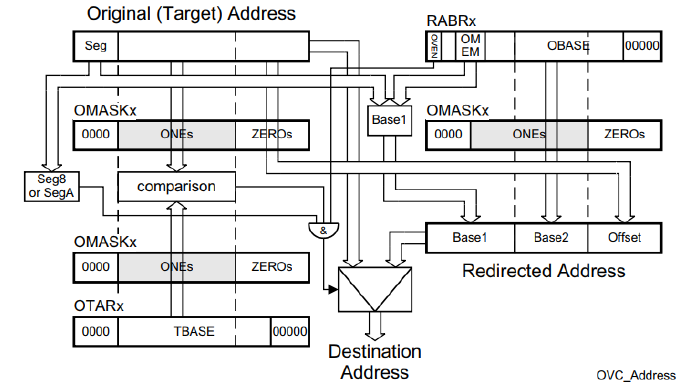
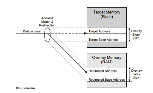
地址访问重映射机制 (OVC)
TriCore内核中的Overlay功能是一种高效的数据访问重定向机制,它允许将程序Flash、在线数据采集空间或EBU (External Bus Unit) 空间的特定数据访问重定向到覆盖存储器中。这些覆盖存储器可以灵活地配置在多个位置,包括本地存储器、仿真存储器、EBU空间或DPSR/PSPR存储器。这种机制的一个重要特点是它只重定向读写数据访问,而不会影响其他操作,并且在执行重定向时不会带来任何性能损失。这种设计特别适用于需要在程序运行时动态修改Flash中存储的测试和标定参数的场景,为实时系统的参数调整和数据采集提供了灵活且高效的解决方案。通过这种方式,开发人员可以在不中断系统运行的情况下,实现对关键参数的实时修改和监控,这在汽车电子等要求严格的嵌入式系统中具有重要的应用价值。
TC397xx的Overlay系统是一个功能强大且灵活的数据访问重定向机制,它能够将对程序Flash、OLDA或外部EBU空间的数据访问重定向到不同位置的覆盖存储器中,包括本地存储器(LMU)、仿真存储器、EBU空间以及DSPR或PSPR存储器。系统支持高达4MB的覆盖存储器地址范围,每个TriCore内核最多可配置32个Overlay块,单个Overlay块大小可从32字节到128KB不等。每个区块都可以独立配置其存储器位置和大小,并且支持通过单次寄存器写入操作同时控制多个区块的启用或禁用。系统还提供了数据缓存的可编程刷新控制,确保覆盖操作与数据加载同步进行。特别值得注意的是,每个处理器核心都配备了独立的Overlay系统,这种设计极大地提高了系统的灵活性和可用性,使其能够满足各种复杂应用场景的需求。
如下图所示,对0x8H段或0xAH段的任何数据访问都会与所有激活的Overlay块进行检查匹配。对于每个激活的区域,系统会将地址位与目标基地址(OTARx)进行比较,这个按位比较由OMASKx寄存器的内容来限定。只有当对应的OMASKx位被设置为1时,相应的地址位才会参与比较。当所有由OMASKx选择的地址位与OTARx寄存器中的对应位相等时,才会触发访问重定向。这种机制确保了精确的地址匹配和灵活的覆盖范围控制。
在TC3xx芯片中,Cache和Overlay的配合使用需要综合考虑性能和可靠性。首先,对于程序缓存(PCACHE)建议保持开启以提高指令访问效率,而数据缓存(DCACHE)则需要根据Overlay的具体使用场景来灵活配置。对于频繁访问但较少更新的Overlay区域,建议开启缓存以提高访问速度;对于需要实时更新的数据区域,可以考虑使用缓存旁路模式以确保数据的实时性。在数据布局方面,应当将频繁访问的数据放在同一Overlay块中,并使块大小尽可能对齐到Cache line,以提高缓存效率。对于多核场景,每个核心都应该有其独立的Overlay配置,避免相互干扰的同时也保证了各个核数据访问时重定向功能的有效性。同时,在进行Overlay数据更新时,需要注意使用DMI提供的缓存刷新控制,确保Cache和内存数据的一致性。此外,还应建立必要的错误处理机制,以应对可能出现的Cache同步或Overlay访问错误。通过这些优化措施,可以充分发挥Cache和Overlay的性能优势,同时保证系统的可靠性。
OVERLAY功能应用示例
使能各核的Overlay 块区。
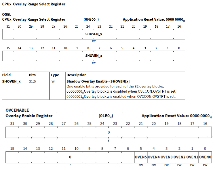
Overlay块区选择寄存器和Overlay功能使能寄存器,每个core都有32个可配置的overlay block,每个block的使能和关闭都对应着寄存器的一个bit。
选取重映射地址:即CPU最终会访问的RAM地址。
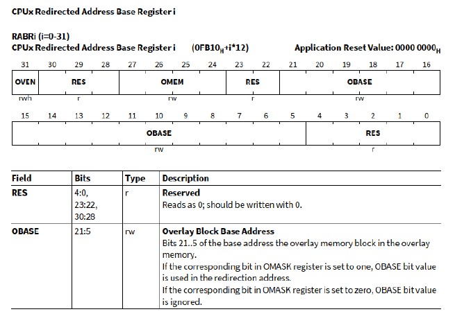
重映射地址基础配置寄存器, OBASE字段用于配置标定区域的基地址。需要在OMEM类型/区域选择的基础上,从其基地址开始偏移的,LMU、DSPR等RAM区域均支持配置。
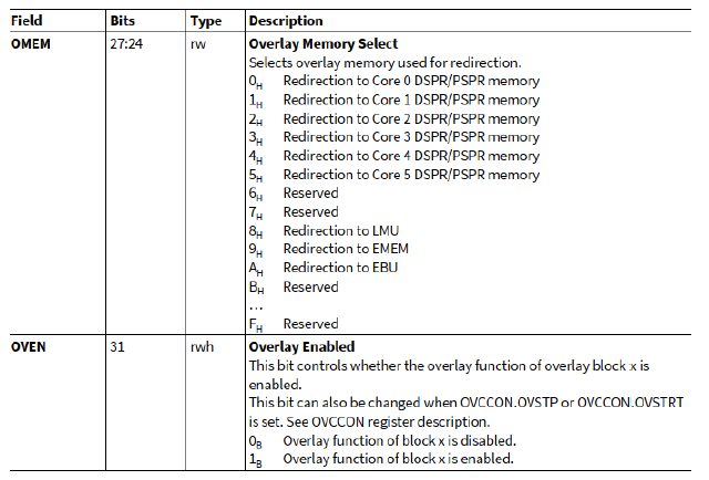
选取目标地址:即CPU访问的数据的DFLASH地址。
重定向目标地址配置寄存器,主要配置的就是需要重映射的地址,0x8h 或 0xAh开头范围内的Flash区域,如PFlash、DFlash和前边提到的外部总线单元地址EBU均可选取配置。
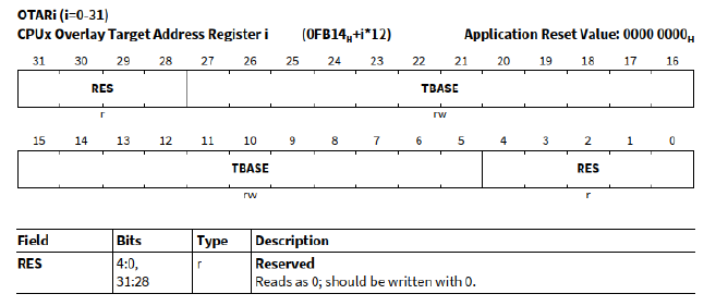
选取Overlay 块区域大小。
重映射掩码寄存器,主要是用来配置重定向区域大小的,共12个bit,如图所示,Overlay 块大小只能是2的n次方的32个字节大小,范围是从32B到128KB。
OVERLAY功能在XCP协议栈中的应用
XCP协议概述
XCP(Universal Measurement and Calibration Protocol)是AUTOSAR中一个重要的标准化协议模块,主要用于ECU的测量和标定。它采用主从架构,其中测试工具(如CANape、INCA等)作为主机,ECU作为从机。XCP支持多种通信方式,最常用的是基于CAN和以太网的传输。
XCP模块的核心功能包括数据测量、在线标定、数据采集(DAQ)、内存读写以及程序下载等。它能够实时监控ECU内部变量,修改标定参数,并支持高速数据采集。在安全性方面,XCP提供了多层次的保护机制,包括标定保护、DAQ保护、编程保护和数据存取保护,确保ECU操作的安全性。
在实际应用中,XCP模块广泛应用于汽车电子开发的多个阶段,特别是在ECU开发、测试和标定过程中。它不仅提供了标准化的接口,确保了不同工具间的兼容性,还支持灵活的配置选项,能够满足不同项目的需求。使用XCP时需要注意合理配置资源、考虑实时性要求、确保数据一致性,并注意带宽限制等因素。总的来说,XCP模块是现代汽车电子开发中不可或缺的工具,能够显著提高开发效率和测试覆盖率。
知从木牛的XCP协议栈产品与OVERLAY 功能的配合
知从木牛产品已实现符合AUTOSAR R20-11规范的XCP协议栈功能,并完成了在TC3XX平台上的移植和应用。标定时性能稳定,且易于集成和使用,能够有效支持汽车电子开发中的调试和标定需求,帮助控制器开发厂商提升效率,降低开发难度。
Data Access Overlay最常见的用途之一便是应用在标定中。标定功能使用的木牛XCP协议栈其本质是为使用者提供了对ECU内部memory的读写机制。读访问保证了标定系统可以从RAM中读取观测量,即测量(measurement);写访问保证了标定系统可以对RAM中的标定量进行数值修改,即标定(calibration)。
Flash区标定数据的修改流程:
1. 上电时完成对各个核所需Overlay块区的初始化并使能需要数据标定的核的Overlay功能,并将划分好的Flash标定区域数据初始化拷贝到Overlay映射的RAM区;
2. 标定时,使得ECU对标定量的访问实际操作的是RAM的Overlay Block区域;
3. 标定结束后,通过上位机工具,如CANape,生成标定好的HEX文件,并刷写进FLASH中完成整个对Flash区参数的标定过程。
关于ZC TC3XX木牛基础软件平台的更多产品
Ø 符合AUTOSAR R20-11版本
Ø ARTOP架构上位机配置工具,最高适配AUTOSAR R20-11版本
Ø 多核操作系统
Ø 通讯协议栈(CAN\LIN)
Ø 诊断协议栈 (UDS\J1939)
Ø 网络管理 (OSEK\AUTOSAR)
Ø 标定协议栈(XCP\CCP)
Ø 存储协议栈
Ø 加密模块(CRYPTO)
Ø 复杂驱动定制开发
Ø 工程服务
知从木牛基础软件产品软件架构
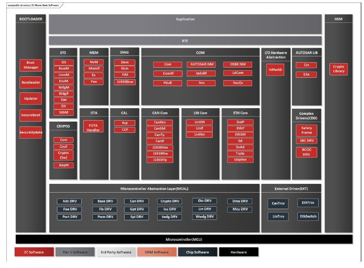
知从木牛基础软件平台架构
为了满足客户的不同项目需求,提高基础软件平台的扩展性,木牛基础软件平台实现了各个模块可配置性,并且实现了配置工具。客户可根据不同需求,在配置工具上完成各个模块的配置工作,可生成配置代码文件,将生成的配置文件集成到工程中即可。
木牛基础软件平台的配置工具是基于Eclipse平台,并基于ARTOP架构,实现AUTOSAR模型和ARXML的解析。除了AUTOSAR标准定义的模块之外,还支持OEM和Tie1厂商二次开发自己的模块。配置完成后,可生成各个模块的配置代码。
汽车在电动化、网联化、智能化的大趋势下,电子电器部件日益增多,电气结构越加复杂,整车开发周期不断缩短。平台化、智能化的基础软件起到至关重要。
知从科技提供基础软件产品的同时,也提供符合ASPICE Level 3流程和功能安全ASIL-D要求的控制器基础软件功能实现的开发服务,SBC芯片、BCCIC芯片各种复杂驱动软件的定制开发。同时,集成知从科技的功能安全产品SafetyFrame,可以满足功能安全要求。
知从科技掌握AUTOSAR平台软件的开发和应用核心技术,提供本地现场支持,质量好,速度快,成本低。
点击下载产品手册